
Please submit your message online and we will contact you as soon as possible!
In-depth understanding of the needs of the market, providing perfect solutions, can better understand customer needs

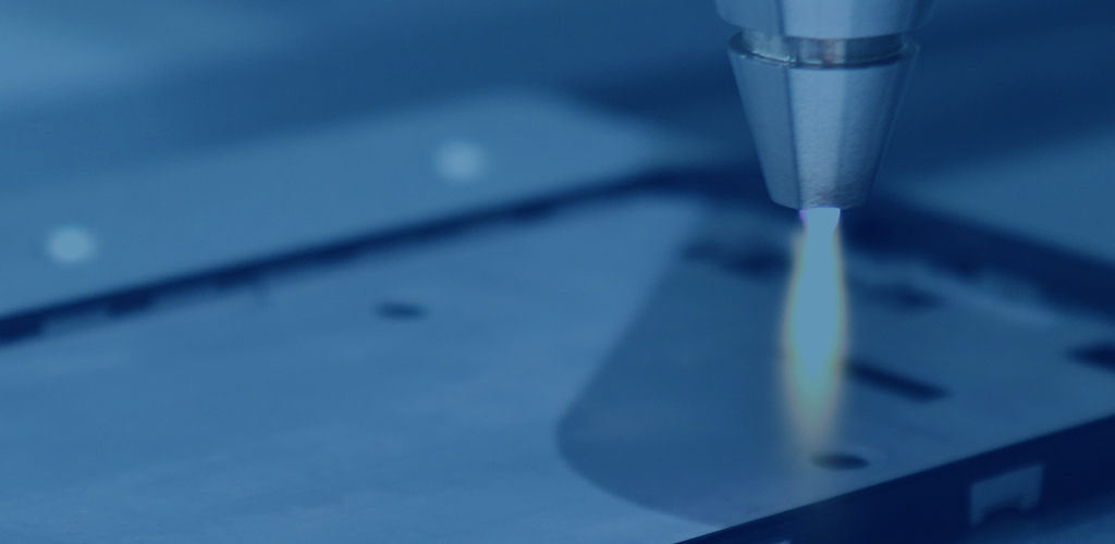
In the LED industry, from packaging to end-user modules, the cleanliness and activation of material surfaces are crucial for device reliability and lifespan. SINDIN plasma technology plays a key role in this process.
Using low-pressure or atmospheric plasma processes, organic residue and fine particles on the material surface are completely removed, while significantly enhancing surface energy. This process not only improves the adhesion between the glue, encapsulation material, and substrate, but also provides stability for subsequent coating, printing, and soldering processes. For LEDs, this translates to a longer lifespan, more stable light color performance, and enhanced environmental adaptability.
Plasma treatment is particularly critical in the MiniLED sector. Due to the smaller size and greater number of MiniLED chips, extremely high demands are placed on placement accuracy and uniformity. Even the slightest contamination can lead to uneven brightness or even failure. SINDIN's plasma cleaning and activation technology ensures highly clean substrate and chip surfaces, improving the consistency of soldering, dispensing, and lamination processes, thereby achieving high-yield production and guaranteeing excellent brightness, contrast, and color reproduction for display products.
In general lighting and display applications, plasma processing makes large-area, high-precision production more controllable and economical.
SINDIN's plasma solutions not only improve the reliability of LED products but also promote greener and more cost-effective manufacturing processes, helping customers achieve the optimal balance between high efficiency and high quality.

Please submit your message online and we will contact you as soon as possible!