Semiconductor
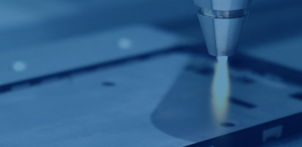
Plasma technology plays a crucial role in semiconductor packaging as a surface activation and cleaning expert, a key process for improving package reliability, yield, and performance. Its core benefits are reflected in the following aspects:
Contaminant and Oxide Removal:
Organic Contaminants: Effectively removes residual organic contaminants such as photoresist, grease, fingerprints, and resin residue from critical locations such as chip surfaces, substrate pads, and lead frames. These contaminants can severely hinder soldering and bonding.
Oxide Layer: Removes the thin oxide layer that naturally forms in air on metal surfaces (such as copper pads and gold wires). This oxide layer can directly lead to poor soldering, cold solder joints, and increased contact resistance. This is a key step in pre-soldering.
Enhancing Surface Energy and Wettability:
Plasma treatment significantly increases the free energy (surface energy) of a material's surface.
Higher surface energy means that molten solder (solder paste, gold-tin alloy, etc.) and packaging materials (EMC, underfill, thermally conductive adhesive, etc.) can better wet (spread) onto the target surface. This directly results in a more uniform and stronger solder/bond interface, reduces voids, and improves mechanical strength and thermal conductivity.
Improving interfacial adhesion:
Excellent adhesion is essential for die attach between the chip and substrate (using DAF or solder), the bonding between the encapsulation compound (EMC) and the chip/substrate/leadframe, and the bonding between the underfill and the chip/substrate.
Plasma treatment cleans and activates the surface, strengthening chemical bonding and physical anchoring at the molecular level, significantly improving the bond strength between dissimilar materials and preventing delamination.
Specific Application Scenarios:
Die Attach Pretreatment:
Cleaning the chip backside and substrate pads (or DAF area) removes organic matter and minor oxides.
Activating the surface ensures perfect wetting and adhesion of the solder or DAF, reducing voids, and improving thermal and electrical conductivity and mechanical strength. Pre-wire Bonding Cleaning:
Cleans chip pads (Al and Cu pads) and leadframe finger solder joints, removing oxide layers (especially copper oxide) and organic contaminants.
Improves pad surface energy, ensuring strong, low-resistance, and highly reliable ball and wedge bonds for gold and copper wires.
Pre-bumping for Flip Chip and Wafer-Level Packaging (WLP):
Cleans chip bumps (solder balls and copper pillars) and substrate pads, removing oxides and contaminants.
Improves surface wettability, ensuring reliable solder joints during reflow, reducing bridging and cold solder joints.
Pre-treatment for Thermocompression Bonding (TCB)/Laser-Assisted Bonding (LAB):
Selectively or globally cleans chip bumps and substrate pads, removing oxides and contaminants from critical areas, creating ideal surface conditions for single-step bonding. Molding Pretreatment:
Cleans and activates all surfaces that will come into contact with the encapsulating compound (EMC), including the substrate, chip, and leadframe.
This significantly improves the adhesion of the EMC to these surfaces, preventing moisture intrusion and interfacial delamination during high/low temperature cycling, thereby enhancing the package's sealing and long-term reliability.
Underfill Pretreatment:
Before dispensing and filling, cleans and activates the chip bottom, substrate surface, and solder ball/bump sides.
This enhances the underfill's flowability and gap wetting properties, ensuring complete fill without voids. It also improves the bond between the underfill and the chip/substrate, effectively dissipating stress and preventing solder joint fatigue failure.
Low-Temperature Processing: Typically causes no damage to heat-sensitive components.
Efficient and Thorough: Capable of processing surfaces with complex geometries (micropores, deep holes, and gaps), removing hard-to-reach contaminants.
Improved Reliability: Fundamentally resolves interface issues, significantly enhancing the package's resistance to moisture, heat, temperature cycling, and mechanical shock.